Description
DFN(PL)2527-10
Pin No
Symbol
Pin Description
1
VDD
Input Pin
2
VDD
Input Pin
3
CE1
Chip Enable Pin 1 ("H" Active)
4
CE2
Chip Enable Pin 2 ("H" Active)
5
CE3
Chip Enable Pin 3 ("H" Active)
6
GND
Ground Pin
7
NC
No Connection
8
VOUT3
Output Pin 3
9
VOUT2
Output Pin 2
10
VOUT1
Output Pin 1
∗) Tab is GND level.(They are connected to the reverse side of this IC.)
The tab is better to be connected to the GND, but leaving it open is also acceptable.The VDD
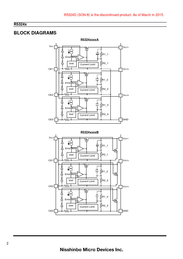
Features
- Supply Current Typ. 90μA (VR1, VR2, VR3).
- Standby Current Typ. 0.1μA.
- Output Current Min. 200mA (VR1), 150mA (VR2), 100mA (VR3).
- Dropout Voltage Typ. 0.23V (VR1) (IOUT=200mA, VOUT=2.8V)
Typ. 0.22V (VR2) (IOUT=150mA, VOUT=2.8V) Typ. 0.15V (VR3) (IOUT=100mA, VOUT=2.8V).
- Ripple Rejection Typ. 70dB (f=1kHz), Typ. 65dB (f=10kHz).
- Input Voltage Range 2.0V to 6.0V.
- Output Voltage Range 1.5V to 4.0V (0.1V steps) (For details, please re.
 R5324K-Nisshinbo.pdf