RP123N
OVERVIEW
No.EA-508-230821
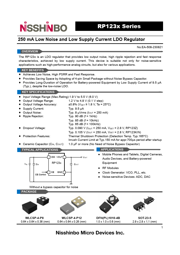
The RP123x is an LDO regulator that provides low output noise, high ripple rejection and fast response characteristics, achieved by low supply current. This device is suitable not only for noise-sensitive applications such as high-performance analog circuits, but also for various applications.
KEY BENEFITS
- Achieves Low Noise, High PSRR and Fast Response.
- Provides Saving Space by Adopting of 4-pin Small Package without Noise Bypass Capacitor.
- Provides Long-Duration of Operation for Battery-powered Equipment by Low Supply Current of 9.5 µA
(Typ.), despite the low-noise LDO.
KEY SPECIFICATIONS
- Input Voltage Range (Max.Rating):1.9 V to 5.5 V (6.0 V)
- Output Voltage Range:
1.2 V to 4.8 V (0.1 V step)
- Output Voltage Accuracy:
- Supply Current:
- Output Noise:
- Ripple Rejection:
±0.8% (VSET ≥ 1.8 V, Ta = 25°C) Typ. 9.5 µA Typ. 8 µVrms (IOUT = 250 m A) Typ. 90 d B (f = 1k Hz)
Typ. 85 d B (f = 10k Hz)
- Dropout Voltage:
Typ. 65 d B (f = 100k Hz) Typ....