2N5401G
Features
- Pb- Free Packages are Available- http://onsemi.
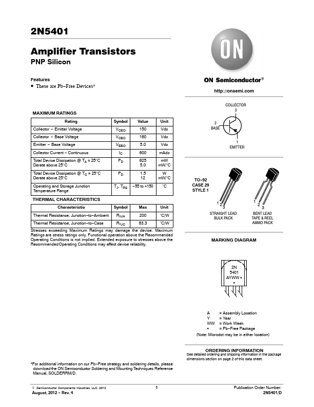
COLLECTOR 3
MAXIMUM RATINGS
Rating Collector
- Emitter Voltage Collector
- Base Voltage Emitter
- Base Voltage Collector Current
- Continuous Total Device Dissipation @ TA = 25°C Derate above 25°C Total Device Dissipation @ TC = 25°C Derate above 25°C Operating and Storage Junction Temperature Range Symbol VCEO VCBO VEBO IC PD 625 5.0 PD 1.5 12 TJ, Tstg
- 55 to +150 Watts m W/°C °C 12 3 m W m W/°C TO- 92 CASE 29 STYLE 1 2N5400 2N5401 120 130 5.0 600 150 160 Unit Vdc Vdc Vdc m Adc 1 EMITTER 2 BASE
Maximum ratings are those values beyond which device damage can occur. Maximum ratings applied to the device are individual stress limit values (not normal operating conditions) and are not valid simultaneously. If these limits are exceeded, device functional operation is not implied, damage may occur and reliability may be affected.
MARKING DIAGRAM
2N 540x AYWWG G
THERMAL CHARACTERISTICS
Characteristic Thermal Resistance, Junction- to-...