Datasheet Details
- Part number
- HC4060AG
- Manufacturer
- ON Semiconductor ↗
- File Size
- 225.84 KB
- Datasheet
- HC4060AG-ONSemiconductor.pdf
- Description
- 14-Stage Binary Ripple Counter
HC4060AG Description
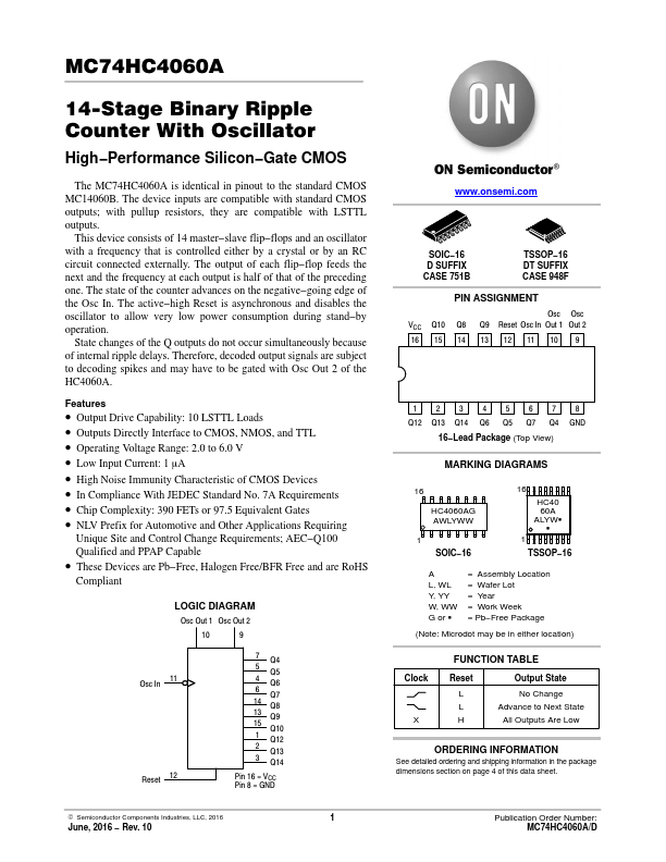
MC74HC4060A 14-Stage Binary Ripple Counter With Oscillator High *Performance Silicon *Gate CMOS The MC74HC4060A is identical in pinout.
HC4060AG Features
* Output Drive Capability: 10 LSTTL Loads
* Outputs Directly Interface to CMOS, NMOS, and TTL
* Operating Voltage Range: 2.0 to 6.0 V
* Low Input Current: 1 mA
* High Noise Immunity Characteristic of CMOS Devices
* In Compliance With JEDEC Standard No.
HC4060AG Applications
* Requiring
Unique Site and Control Change Requirements; AEC
* Q100 Qualified and PPAP Capable
* These Devices are Pb
* Free, Halogen Free/BFR Free and are RoHS
Compliant
LOGIC DIAGRAM
Osc Out 1 Osc Out 2
10
9
Osc In 11 Reset 12
7 Q4 5 Q5 4 Q6 6 Q7 14 Q8 13 Q9 15 Q10 1 Q12 2
📁 Related Datasheet
📌 All Tags