Datasheet Details
| Part number | NCP4547 |
|---|---|
| Manufacturer | ON Semiconductor ↗ |
| File Size | 244.17 KB |
| Description | Advanced Load Management |
| Datasheet |
 NCP4547-ONSemiconductor.pdf NCP4547-ONSemiconductor.pdf
|
| Part number | NCP4547 |
|---|---|
| Manufacturer | ON Semiconductor ↗ |
| File Size | 244.17 KB |
| Description | Advanced Load Management |
| Datasheet |
NCP4547-ONSemiconductor.pdf
|
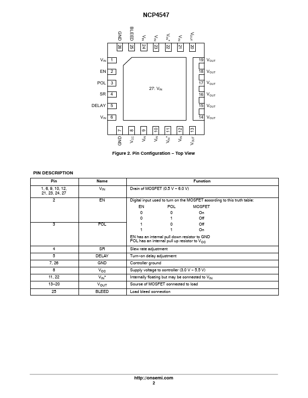
Pin 1, 6, 9, 10, 12, 21, 23, 24, 27 2 3 4 5 7, 26 8 11, 22 13 20 25 Figure 2. Pin Configuration Top View Name VIN EN POL SR DELAY GND VCC VIN VOUT BLEED Function Drain of MOSFET (0.5 V 6.0 V) Digital input used to turn on the MOSFET according to this truth table: EN POL MOSFET 0 0 On 0 1 Off 1 0 Off 1 1 On EN has an internal pull down resistor to GND POL has an internal pull up resistor to VCC Slew rate adjustment Turn on delay adjustment C
📁 NCP4547 Similar Datasheet