Datasheet Details
| Part number | NCP6361 |
|---|---|
| Manufacturer | ON Semiconductor |
| File Size | 1.23 MB |
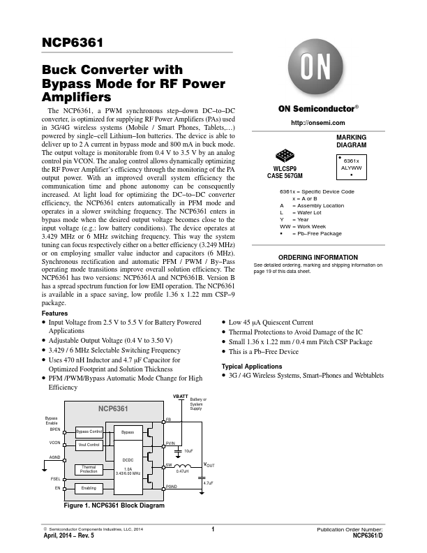
| Description | Buck Converter |
| Datasheet |
 NCP6361-ONSemiconductor.pdf NCP6361-ONSemiconductor.pdf
|
|
|
The NCP6361 by ON Semiconductor is a Buck Converter. Below is the official datasheet preview.
| Part number | NCP6361 |
|---|---|
| Manufacturer | ON Semiconductor |
| File Size | 1.23 MB |
| Description | Buck Converter |
| Datasheet |
NCP6361-ONSemiconductor.pdf
|
|
|
|
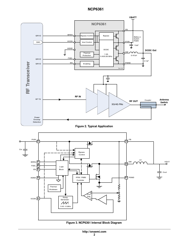
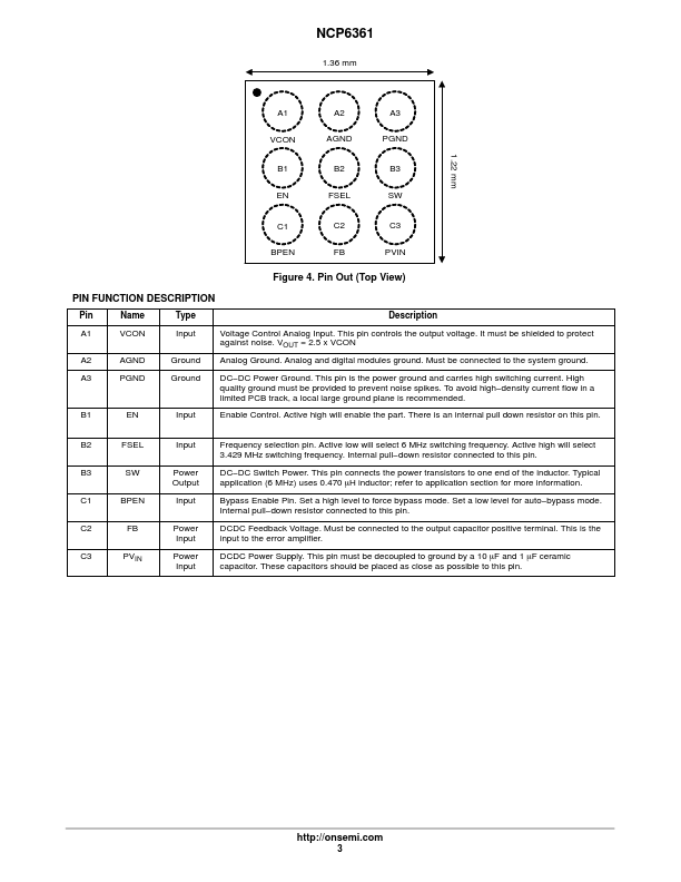
Pin Name Type Description A1 VCON Input Voltage Control Analog Input.This pin controls the output voltage.It must be shielded to protect against noise.VOUT = 2.5 x VCON A2 AGND Ground Analog Ground.Analog and digital modules ground.Must be connected to the system ground.A3 PGND Ground DC DC Power Ground. density current fl
📁 NCP6361 Similar Datasheet