Description
Pin
Function
Description
3
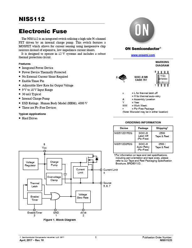
Enable/Timer A high level signal on this pin allows the device to begin operation.Connection of a capacitor will delay
turn on for timing purposes.A low input signal inhibits the operation.1
Ground
Negative input voltage to the device.This is used as the internal reference for the IC.4 5,6,7
ILimit Source
A resistor between this pin and the source pin sets the current limit level.Source of power FET, which is also the switching node for the load.2
Features
- a MOSFET which allows for current sensing using inexpensive chip resistors instead of expensive, low impedance current shunts. It is designed to operate in 12 V systems and includes a robust thermal protection circuit. Features.
- Integrated Power Device.
- Power Device Thermally Protected.
- No External Current Shunt Required.
- Enable/Timer Pin.
- Adjustable Slew Rate for Output Voltage.
- 9 V to 18 V Input Range.
- 30 mW Typical.
- Inter.
 NIS5112_ONSemiconductor.pdf