Datasheet Details
| Part number | SCV8163 |
|---|---|
| Manufacturer | ON Semiconductor ↗ |
| File Size | 1.01 MB |
| Description | Ultra-Low Noise and High PSRR LDO Regulator |
| Datasheet |
 SCV8163-ONSemiconductor.pdf SCV8163-ONSemiconductor.pdf
|
| Part number | SCV8163 |
|---|---|
| Manufacturer | ON Semiconductor ↗ |
| File Size | 1.01 MB |
| Description | Ultra-Low Noise and High PSRR LDO Regulator |
| Datasheet |
SCV8163-ONSemiconductor.pdf
|
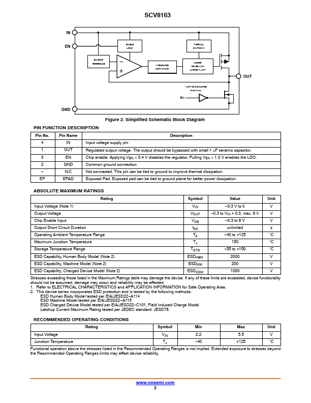
Pin No. N/C Not connected.This pin can be tied to ground to improve thermal dissipation.EP EPAD Exposed Pad.Exposed pad can be tied to ground plane for better power dissipation.ABSOLUTE
📁 SCV8163 Similar Datasheet