PG 9732-D om
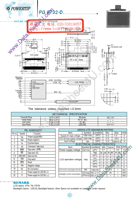
OUTLINE DIMENSION & BLOCK DIAGRAM
1.0
41 1.5
1.7
1.5
1 11.7
6.0
DB7(SCL) DB6(SI) DB0 Vss Vdd Vo Ao
R W(WR)
COM 1(I-CON) LCD CONTROLLER LSI SED1530 COM 32
LCD PANEL
E(RD) CS1 RES Vee A K
SEG 97
The tolerance unless classified
Overall Size View Area Dot Size Dot Pitch 42.0 x 39.9 36.0 x 21.0 0.28 x 0.39 0.32 x 0.43
PIN ASSIGNMENT
Pin no. 1 2 3 4 5 6 7-14 15 16 17 18 19 20 Symbol Vss Vdd Vo A0 WR RD DB0-DB7 CS1 RES Vee NC A K
Function Power supply(GND) Power supply(+) Contrast Adjust Command / data input Data write / (R/W) Data read / (E) Data bus line Chip select Reset Negative voltage No Connection Power supply for LED B/L (+) Power supply for LED B/L ( )
w
w
w
t a .D
MECHANICAL SPECIFICATION
Module W /O B/L EL B/L LED B/L H2 / H1 / / 3.9 / 4.
 PG9732_D Datasheet