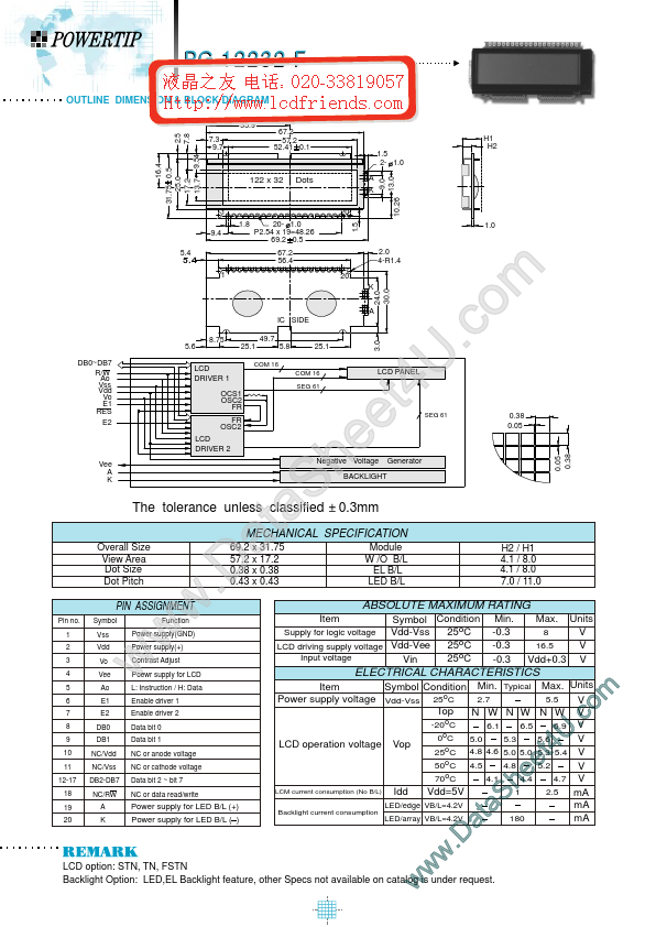
Click to expand full text
PG 12232-F
OUTLINE DIMENSION & BLOCK DIAGRAM
35.9 2.5 7.8 7.3 9.7 67.2 57.2 52.41 0.1 1.5 2- 1.0 9.0 13.0
H1 H2
16.4 31.75 0.5 25.0 17.2 13.7 9.54
122 x 32
Dots
A K
1 1.8 9.4 5.4 1 20- 1.0 P2.54 x 19=48.26 69.2 0.5 67.2 56.4
20 1.5
10.26
1.0
DB0~DB7 R/W Ao Vss Vdd Vo E1 RES E2
Vee A K
The tolerance unless classified
Overall Size View Area Dot Size Dot Pitch 69.2 x 31.75 57.2 x 17.2 0.38 x 0.38 0.43 x 0.43
PIN ASSIGNMENT
Pin no. 1 2 3 4 5 6 7 8 9 10 11 12-17 18 19 20 Symbol Vss Vdd Vo Vee Ao E1 E2 DB0 DB1 NC/Vdd NC/Vss DB2-DB7 NC/RW A K
Function Power supply(GND) Power supply(+) Contrast Adjust
Poewr supply for LCD Enable driver 1 Enable driver 2 Data bit 0 Data bit 1 NC or anode voltage
L: Instruction / H: Data
m o .c U 4 t e e h S a t a .D w w w
20 A IC SIDE 5.6 25.1 5.