Datasheet Details
| Part number | AN5392FBQ |
|---|---|
| Manufacturer | Panasonic Semiconductor |
| File Size | 203.37 KB |
| Description | Luminance and color difference drive/cutoff signal processor |
| Datasheet |
 AN5392FBQ Datasheet AN5392FBQ Datasheet
|
|
|
| Part number | AN5392FBQ |
|---|---|
| Manufacturer | Panasonic Semiconductor |
| File Size | 203.37 KB |
| Description | Luminance and color difference drive/cutoff signal processor |
| Datasheet |
AN5392FBQ Datasheet
|
|
|
|
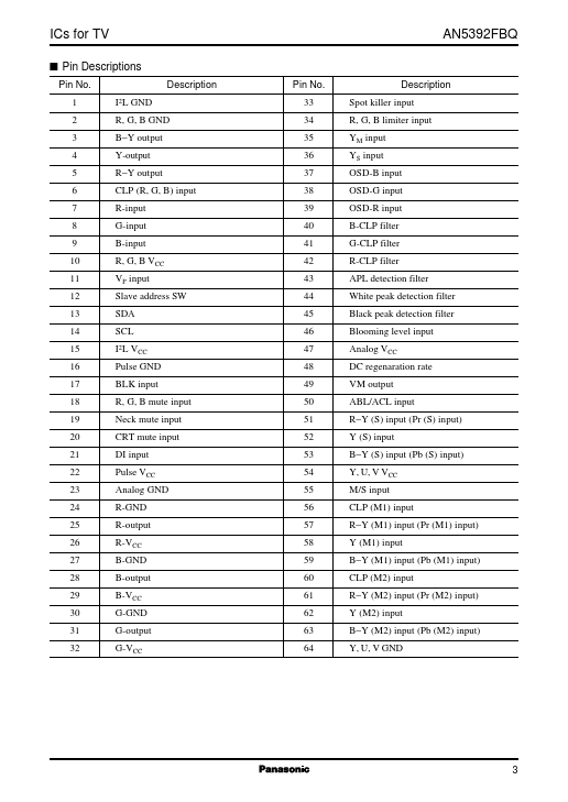
Pin No.
📁 Similar Datasheet