Datasheet Details
| Part number | AN7118S |
|---|---|
| Manufacturer | Panasonic Semiconductor |
| File Size | 33.20 KB |
| Description | Low Voltage Dual 35mW Audio Power Amplifier |
| Datasheet |
 AN7118S Datasheet AN7118S Datasheet
|
|
|
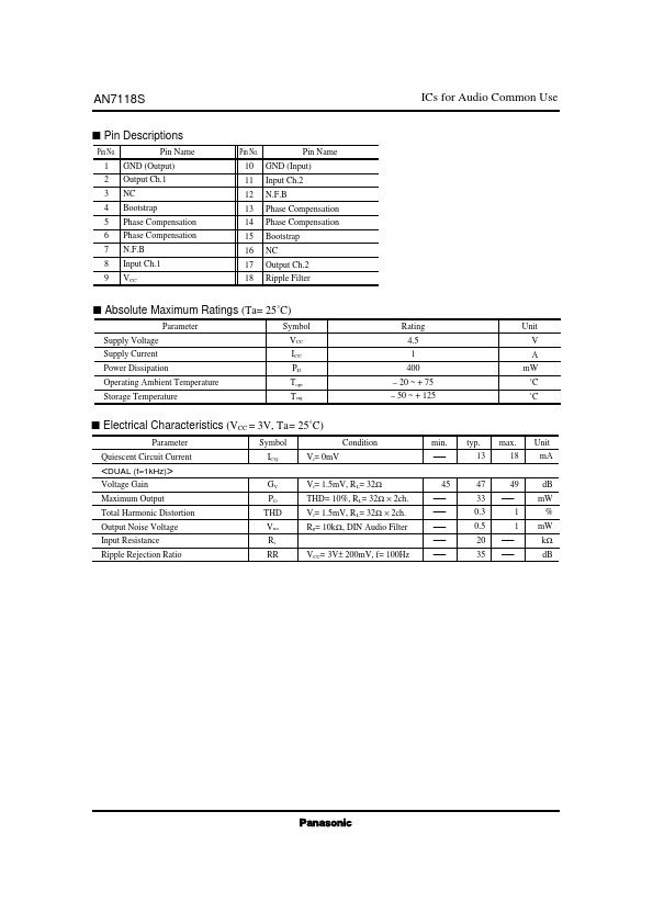
Pin No.
1 2 3 4 5 6 7 8 9 Pin Name GND (Output) Output Ch.1 NC Bootstrap Phase Compensation Phase Compensation N.F.B Input Ch.1 VCC Pin No.
| Part number | AN7118S |
|---|---|
| Manufacturer | Panasonic Semiconductor |
| File Size | 33.20 KB |
| Description | Low Voltage Dual 35mW Audio Power Amplifier |
| Datasheet |
AN7118S Datasheet
|
|
|
|