PJM250N40TO
Features
- High density cell design for ultra low RDS(on)
- Low RDS(ON) and Gate Charge
- Excellent package for good heat dissipation
Applications
- Power switching application
- Hard switched and high frequency circuits
- Uninterruptible power supply
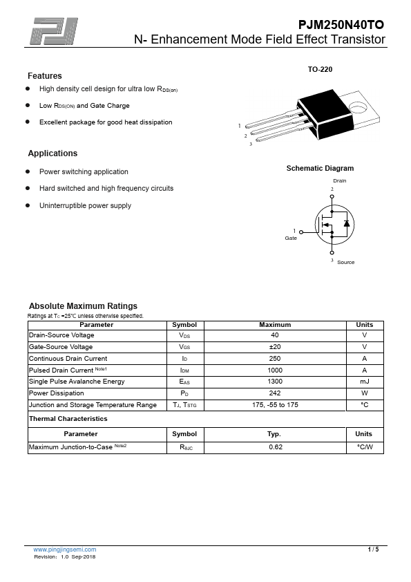
TO-220
2 3
Schematic Diagram
Drain 2
1 Gate
3 Source
Absolute Maximum Ratings
Ratings at TC =25℃ unless otherwise specified.
Parameter Drain-Source Voltage Gate-Source Voltage Continuous Drain Current Pulsed Drain Current Note1 Single Pulse Avalanche Energy Power Dissipation Junction and Storage Temperature Range
Thermal Characteristics
Parameter
Maximum Junction-to-Case Note2
Symbol VDS VGS ID IDM EAS PD
TJ, TSTG
Symbol RθJC
Maximum 40 ±20 250
1000 1300 242 175, -55 to 175
Typ. 0.62
Units V V A A m J W °C
Units °C/W
.pingjingsemi. Revision:1.0 Sep-2018
1/5
PJM250N40TO N- Enhancement Mode Field Effect Transistor
Electrical Characteristics...