PDNM8PN30V12
Description
The MOSFET provide excellent RDS(ON) with low gate charge. This device is suitable for use as a wide variety of applications.
VDS(V) 30
MOSFET Product Summary
RDS(on)(mΩ) <15@ VGS=10V <20@ VGS=4.5V
ID(A) 12
Application
- Power switching application
- Hard switched and high frequency circuits
- Uninterruptible power supply
PDNM8PN30V12 Dual N-Channel MOSFET
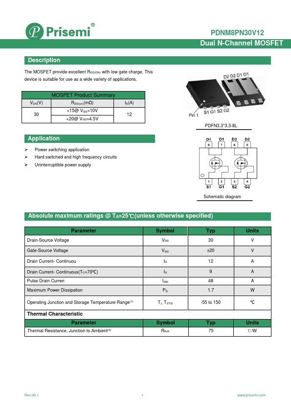
PDFN3.3- 3.3-8L
Schematic diagram
Absolute maximum ratings @ TA=25℃(unless otherwise specified)
Parameter
Drain-Source Voltage Gate-Source Voltage Drain Current- Continuou Drain Current- Continuous(TC=70℃) Pulse Drain Curren Maximum Power Dissipation
Operating Junction and Storage Temperature Range(1)
Thermal Characteristic Parameter
Thermal Resistance, Junction to Ambient(2)
Symbol
VDS VGS ID ID IDM PD
TJ, TSTG
Symbol
RθJA
Typ
30 ±20 12
9 48 1.7
-55 to 150
Typ
Units
V V A A A W
℃
Units
℃/W
Rev.06.1
1 .prisemi.
Dual N-Channel MOSFET
Electrical characteristics per line @25℃(unless otherwise...