PNM6N20V10E
Description
The MOSFET provide the best bination of fast switching, low on-resistance and cost-effectiveness.
VDS(V) 20
MOSFET Product Summary
RDS(on)(mΩ)
ID(A)
7.5 @ VGS=4.5V
PNM6N20V10E N-Channel MOSFET
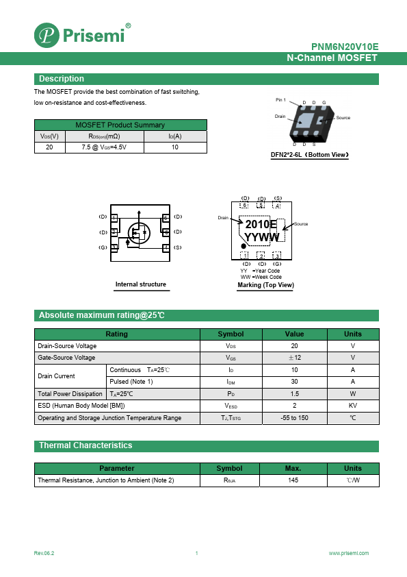
Pin 1 Drain
DDG Source
DFN2- 2-6L(Bottom View)
(D) 1 (D) 2 (G) 3
6 (D) 5 (D) 4 (S)
Internal structure
Absolute maximum rating@25℃
Rating
Drain-Source Voltage
Gate-Source Voltage
Drain Current
Continuous TA=25℃ Pulsed (Note 1)
Total Power Dissipation TA=25℃
ESD (Human Body Model [BM])
Operating and Storage Junction Temperature Range
Thermal Characteristics
Parameter
Thermal Resistance, Junction to Ambient (Note 2)
(D) (D) (S) 654
2010EDrain
Source
YYWW
(D) (D) (G) YY =Year Code WW =Week Code
Marking (Top View)
Symbol
VDS VGS ID IDM PD VESD TJ,TSTG
Value
20 ±12
10 30 1.5 2 -55 to...