PPM6N12V10
Description
The enhancement mode MOS is extremely high density cell and low on-resistance.
PPM6N12V10 P-Channel MOSFET
VDS(V) -12
MOSFET Product Summary
RDS(on)(mΩ)
ID(A)
12 @ VGS=-4.5V
-10
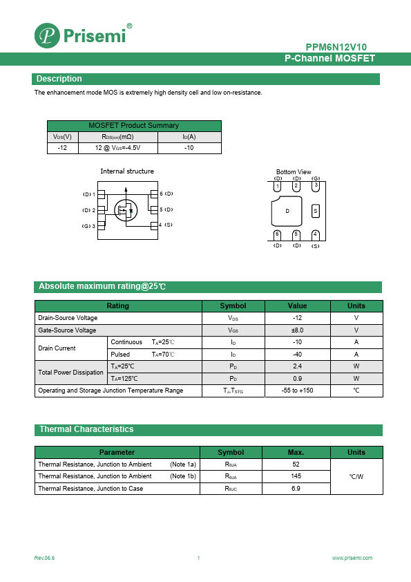
Internal structure
(D)1 (D)2 (G)3
6(D) 5(D) 4(S)
Bottom View
(D) (D) (G)
(D) (D) (S)
Absolute maximum rating@25℃
Rating
Drain-Source Voltage
Gate-Source Voltage
Drain Current
Continuous Pulsed
TA=25℃ TA=70℃
TA=25℃ Total Power Dissipation
TA=125℃
Operating and Storage Junction Temperature Range
Symbol
VDS VGS ID ID PD PD TJ,TSTG
Thermal Characteristics
Parameter
Thermal Resistance, Junction to Ambient Thermal Resistance, Junction to Ambient Thermal Resistance, Junction to Case
(Note 1a) (Note 1b)
Symbol
RθJA RθJA RθJC
Value
-12 ±8.0 -10 -40 2.4 0.9 -55 to +150
Units
V V A A W W...