RP111N071D
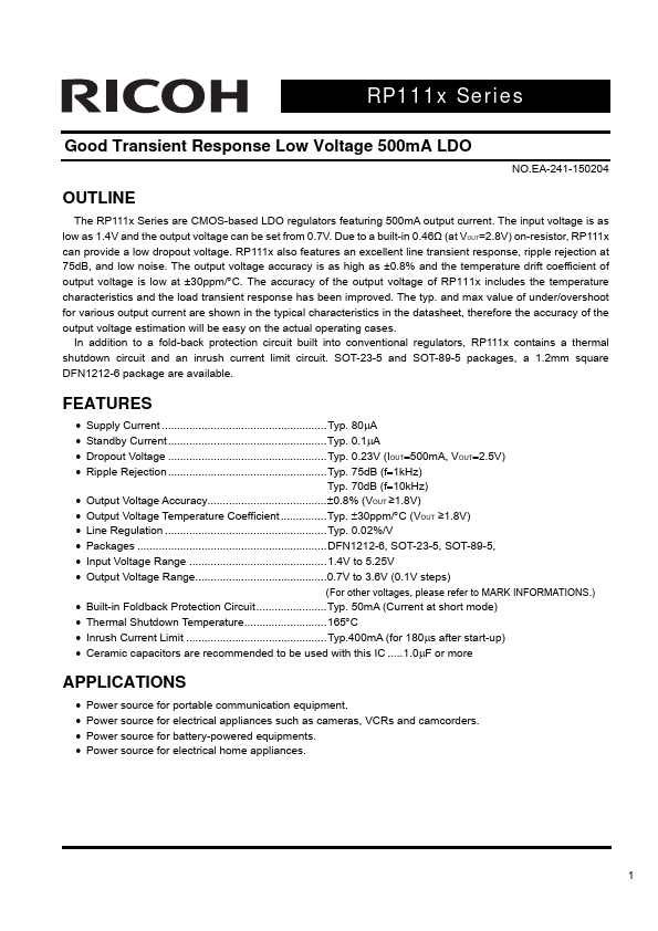
features an excellent line transient response, ripple rejection at 75d B, and low noise. The output voltage accuracy is as high as ±0.8% and the temperature drift coefficient of output voltage is low at ±30ppm/C. The accuracy of the output voltage of RP111x includes the temperature characteristics and the load transient response has been improved. The typ. and max value of under/overshoot for various output current are shown in the typical characteristics in the datasheet, therefore the accuracy of the output voltage estimation will be easy on the actual operating cases.
In addition to a fold-back protection circuit built into conventional regulators, RP111x contains a thermal shutdown circuit and an inrush current limit circuit. SOT-23-5 and SOT-89-5 packages, a 1.2mm square DFN1212-6 package are available.
FEATURES
- Supply Current Typ. 80A
- Standby Current Typ. 0.1A
-...


