Datasheet4U Logo Datasheet4U.com

9SBV0802

Dual 1:4 Fanout Buffer

9SBV0802 Features

* Eight 1

* 48MHz 1.05V LVCMOS outputs Key Specifications

* Additive cycle-to-cycle jitter < 8ps

* Output-to-output skew within a bank < 50ps

* Output-to-output skew between banks < 100ps Block Diagram vOE_07# vOE_2345# ICLKA_1.05 ICLKB_1.05 VREF_1.05 vOE_16

9SBV0802 General Description

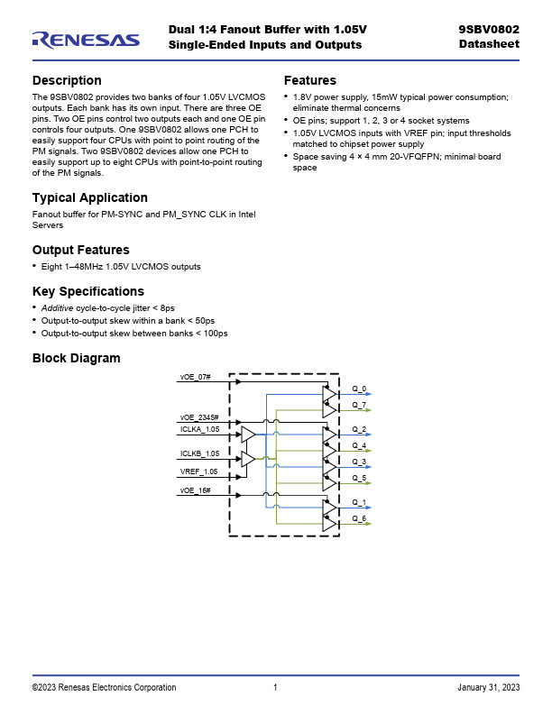
The 9SBV0802 provides two banks of four 1.05V LVCMOS outputs. Each bank has its own input. There are three OE pins. Two OE pins control two outputs each and one OE pin controls four outputs. One 9SBV0802 allows one PCH to easily support four CPUs with point to point routing of the PM signals. Two 9S.

9SBV0802 Datasheet (583.81 KB)

Preview of 9SBV0802 PDF

Datasheet Details

Part number:

9SBV0802

Manufacturer:

Renesas ↗

File Size:

583.81 KB

Description:

Dual 1:4 fanout buffer.

📁 Related Datasheet

9SBV0802 - Dual 1:4 Fanout Buffer (IDT)
Dual 1:4 Fanout Buffer with 1.05V Single-Ended Inputs and Outputs 9SBV0802 DATASHEET General Description The 9SBV0802 provides two banks of four 1.0.

9SQ445 - Clock Generator (Renesas)
CK440Q Lite PCIe Gen6 Clock Generator 9SQ445 Datasheet Description The 9SQ445 is a single-chip, PCIe Gen6 clock synthesizer providing a subset of th.

9SQL4952 - Gen1-5 and UPI Clock Generator (Renesas)
3.3V PCIe® Gen1–5 and UPI Clock Generator Family 9SQL4952/9SQL4954/ 9SQL4958 Datasheet Description The 9SQL4952/9SQL4954/9SQL4958 devices prise a.

9SQL4952C - Gen1-5 and UPI Clock Generator (Renesas)
3.3V PCIe® Gen1–5 and UPI Clock Generator Family 9SQL4952/9SQL4954/ 9SQL4958 Datasheet Description The 9SQL4952/9SQL4954/9SQL4958 devices prise a.

9SQL4954 - Gen1-5 and UPI Clock Generator (Renesas)
3.3V PCIe® Gen1–5 and UPI Clock Generator Family 9SQL4952/9SQL4954/ 9SQL4958 Datasheet Description The 9SQL4952/9SQL4954/9SQL4958 devices prise a.

9SQL4954C - Gen1-5 and UPI Clock Generator (Renesas)
3.3V PCIe® Gen1–5 and UPI Clock Generator Family 9SQL4952/9SQL4954/ 9SQL4958 Datasheet Description The 9SQL4952/9SQL4954/9SQL4958 devices prise a.

9SQL4958 - Gen1-5 and UPI Clock Generator (Renesas)
3.3V PCIe® Gen1–5 and UPI Clock Generator Family 9SQL4952/9SQL4954/ 9SQL4958 Datasheet Description The 9SQL4952/9SQL4954/9SQL4958 devices prise a.

9SQL4958C - Gen1-5 and UPI Clock Generator (Renesas)
3.3V PCIe® Gen1–5 and UPI Clock Generator Family 9SQL4952/9SQL4954/ 9SQL4958 Datasheet Description The 9SQL4952/9SQL4954/9SQL4958 devices prise a.

TAGS

9SBV0802 Dual Fanout Buffer Renesas

Image Gallery

9SBV0802 Datasheet Preview Page 2 9SBV0802 Datasheet Preview Page 3

9SBV0802 Distributor