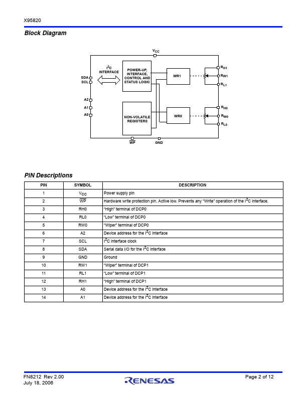
Description
PIN SYMBOL 1 VCC 2 WP 3 RH0 4 RL0 5 RW0 6 A2 7 SCL 8 SDA 9 GND 10 RW1 11 RL1 12 RH1 13 A0 14 A1
DESCRIPTION Power supply pin Hardware write protection pin.Active low.Prevents any “Write” operation of the I2C interface.“High” terminal of DCP0 “Low” terminal of DCP0 “Wiper” terminal of DCP0 Device address for the I2C interface I2C interface clock Serial data I/O for the I2C interface Ground “Wiper” terminal of DCP1 “Low” terminal of DCP1 “High” terminal of DCP1 Device address for the I2C inte
Features
- Two potentiometers in one package.
- 256 resistor taps-0.4% resolution.
- I2C serial interface
- Three address pins, up to eight devices/bus.
- Wiper resistance: 70 typical @ 3.3V.
- Non-volatile storage of wiper position.
- Standby current < 5µA max.
- Power supply: 2.7V to 5.5V.
- 50k, 10k total resistance.
- High reliability
- Endurance: 150,000 data changes per bit per register - Register data retention: 50 years @ T 75°C.
 X95820-Renesas.pdf