Datasheet Details
| Part number | 9729K |
|---|---|
| Manufacturer | ROHM |
| File Size | 144.99 KB |
| Description | BU9729K |
| Datasheet |
 9729K_Rohm.pdf 9729K_Rohm.pdf
|
| Part number | 9729K |
|---|---|
| Manufacturer | ROHM |
| File Size | 144.99 KB |
| Description | BU9729K |
| Datasheet |
9729K_Rohm.pdf
|
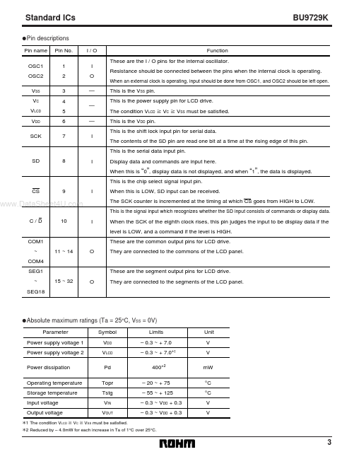
Pin name OSC1 OSC2 VSS VC VLCD VDD SCK Pin No. I I/O I O Function These are the I / O pins for the internal oscillator.
📁 9729K Similar Datasheet