1) Can drive up to 200 mA. 2) Controlling the strobe terminal with the drive timing pulse enables current to be reduced when drive is not being carried out. 3) Using the data output terminal for the next data input enables cascade connections. 4) The digital ground and power ground are separated. 5) TTL and CMOS drive possible.
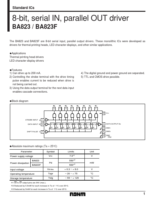
Block diagram
O0 12 O1 11 O2 10 O3 9 O4 8 O5 7 O6 6 O7 5 16 VCC STROBE INPUT S 1 D Q C SHIFT PULSE C 2 D Q C D Q C D Q C D Q C D Q C D Q C D Q C 3 DA.