RK3055E
Key Features
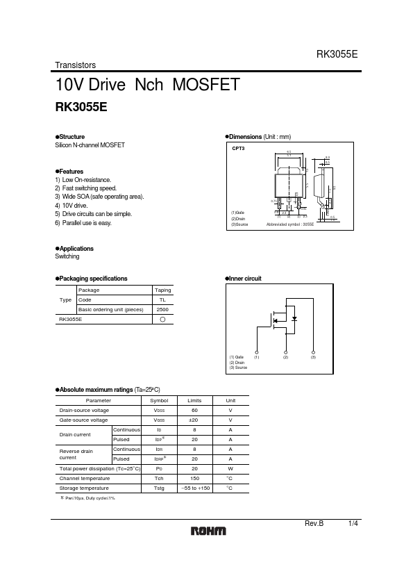
- 8Min. 2.5 (1)Gate (2)Drain (3)Source
- 9 2.3 (1) (2) (3) 2.3
- 0 Abbreviated symbol : 3055E zInner circuit (1) Gate (1) (2) Drain (3) Source zAbsolute maximum ratings (Ta=25°C) Parameter Symbol Limits Unit Drain-source voltage VDSS 60 V Gate-source voltage VGSS ±20 V Continuous ID 8 A Drain current Pulsed IDP∗ 20 A Reverse drain Continuous IDR 8 A current Pulsed IDRP∗ 20 A Total power dissipation (Tc=25°C) PD 20 W Channel temperature Tch 150 °C Storage temperature ∗ Pw≤10µs, Duty cycle≤1% Tstg -55 to +150 °C (2) (3) Rev.B 1/4 Transistors RK3055E zElectrical characteristics (Ta=25°C) Parameter Symbol Min. Typ. Max. Unit Test Conditions Gate-source leakage IGSS - Drain-source breakdown voltage V(BR)DSS 60 Zero gate voltage drain current IDSS - Gate threshold voltage VGS(th)
- 0 Static drain-source on-state resistance Forward transfer admittance RDS(on) - Yfs ∗ 4.0 Input capacitance Ciss - Output capacitance Coss - Reverse transfer capacitance Crss - Turn-on delay time td(on) - Rise time tr - Turn-off delay time td(off) - Fall time ∗ Pw ≤ 300µs, Duty cycle ≤ 1% tf - - ±100 - - - 10 -
- 5 - 0.15 - - 520 - 240 - 100 -
- 0 - 20 - 50 - 20 - nA VGS=±20V, VDS=0V V ID=1mA, VGS=0V µA VDS=60V, VGS=0V V VDS=10V, ID=1mA Ω ID=4A, VGS=10V S ID=4A, VDS=15V pF VDS=10V pF VG=0V pF f=1MHz ns ID=2.5A, VDD 30V ns VGS=10V ns RL=12Ω ns RG=10Ω