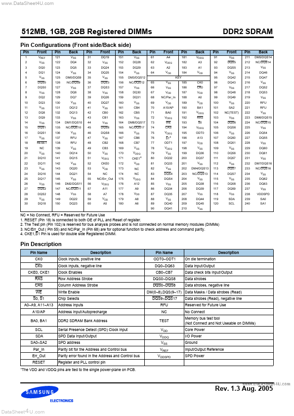
Description
Pin Name CK0 CK0 CKE0, CKE1 RAS CAS WE S0, S1 A0~A9, A11~A13 A10/AP BA0, BA1 SCL SDA SA0~SA2 Par_In Err_Out RESET Description Clock Inputs, positive line Clock inputs, negative line Clock Enables Row Address Strobe Column Address Strobe Write Enable Chip Selects Address Inputs Address Input/Autoprecharge DDR2 SDRAM Bank Address Serial Presence Detect (SPD) Clock Input SPD Data Input/Output SPD address Parity bit for the Address and Control bus Parity error found in the Address and Control bus Re
Features
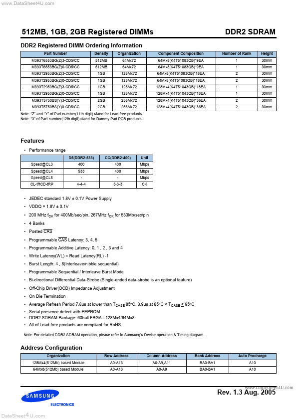
- Performance range
D5(DDR2-533) Speed@CL3 Speed@CL4 Speed@CL5 CL-tRCD-tRP 400 533 4-4-4 CC(DDR2-400) 400 400 3-3-3 Unit Mbps Mbps Mbps CK.
- JEDEC standard 1.8V ± 0.1V Power Supply.
- VDDQ = 1.8V ± 0.1V.
- 200 MHz fCK for 400Mb/sec/pin, 267MHz fCK for 533Mb/sec/pin.
- 4 Banks.
- Posted CAS.
- Programmable CAS Latency: 3, 4, 5.
- Programmable Additive Latency: 0, 1 , 2 , 3 and 4.
- Write Latency(WL) = Read Latency(RL) -1.
 M393T2950BG_SAMSUNG.pdf