Datasheet Details
- Part number
- M8813F1W
- Manufacturer
- STMicroelectronics ↗
- File Size
- 54.24 KB
- Datasheet
- M8813F1W_STMicroelectronics.pdf
- Description
- In-System Programmable ISP Multiple-Memory/Logic
M8813F1W Description
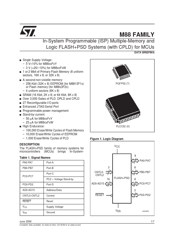
M88 FAMILY In-System Programmable (ISP) Multiple-Memory and Logic FLASH+PSD Systems (with CPLD) for MCUs DATA BRIEFING s s Single Supply Voltage:
M8813F1W Features
* an optimized Macrocell logic architecture. The Macrocell was created to address the unique requirements of embedded system designs. It allows direct connection between the system address/data bus, and the internal FLASH+PSD
Table 2. Product Range1
Part Number M8813F1Y M8813F2Y M8834F2Y M8813F1W M88
📁 Related Datasheet
📌 All Tags
M8813F1W Stock/Price