STW10NB60
DESCRIPTION
Using the latest high voltage MESH OVERLAY™ process, STMicroelectronics has designed an advanced family of power MOSFETs with outstanding performances. The new patent pending strip layout coupled with the pany’s proprietary edge termination structure, gives the lowest RDS(on) per area, exceptional avalanche and dv/dt capabilities and unrivalled gate charge and switching characteristics. APPLICATIONS SWITCH MODE POWER SUPPLIES (SMPS) s DC-AC CONVERTERS FOR WELDING EQUIPMENT AND UNINTERRUPTIBLE POWER SUPPLIES AND MOTOR DRIVE s HIGH CURRENT, HIGH SPEED SWITCHING s
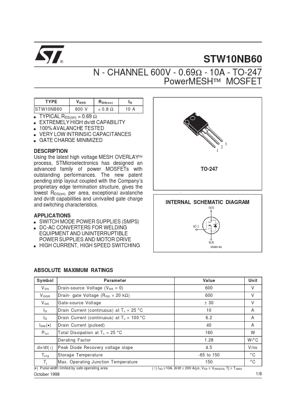
TO-247
INTERNAL SCHEMATIC DIAGRAM
ABSOLUTE MAXIMUM RATINGS
Symbol V DS V DGR V GS ID ID I DM (
- ) P tot dv/dt( 1 ) Ts tg Tj Parameter Drain-source Voltage (VGS = 0) Drain- gate Voltage (R GS = 20 k Ω ) G ate-source Voltage Drain Current (continuous) at Tc = 25 C Drain Current (continuous) at Tc = 100 C Drain Current (pulsed) T otal Dissipation at Tc = 25 C Derating Factor Peak Diode Recovery voltage slope...