STW10NC70Z
DESCRIPTION
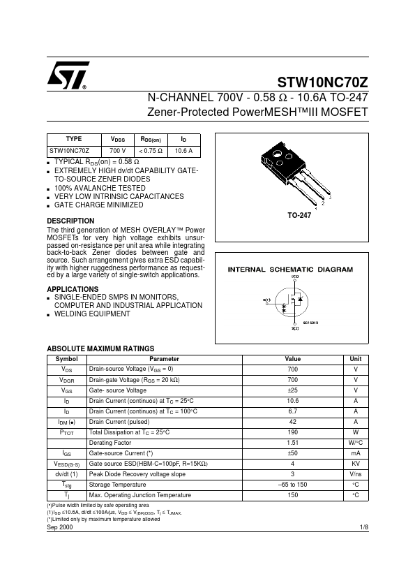
The third generation of MESH OVERLAY ™ Power MOSFETs for very high voltage exhibits unsurpassed on-resistance per unit area while integrating back-to-back Zener diodes between gate and source. Such arrangement gives extra ESD capability with higher ruggedness performance as requested by a large variety of single-switch applications. APPLICATIONS s SINGLE-ENDED SMPS IN MONITORS, PUTER AND INDUSTRIAL APPLICATION s WELDING EQUIPMENT
ABSOLUTE MAXIMUM RATINGS
Symbol VDS VDGR VGS ID ID IDM (q ) PTOT IGS VESD(G-S) dv/dt (1) Tstg Tj Parameter Drain-source Voltage (VGS = 0) Drain-gate Voltage (RGS = 20 kΩ) Gate- source Voltage Drain Current (continuos) at TC = 25°C Drain Current (continuos) at TC = 100°C Drain Current (pulsed) Total Dissipation at TC = 25°C Derating Factor Gate-source Current (- ) Gate source ESD(HBM-C=100p F, R=15KΩ) Peak Diode Recovery voltage slope Storage Temperature Max. Operating Junction Temperature Value 700 700 ±25 10.6 6.7 42 190 1.51 ±50 4 3
- 65 to 150...