STY140NS10
DESCRIPTION
Using the latest high voltage MESH OVERLAY™ process, STMicroelectronics has designed an advanced family of power MOSFETs with outstanding performances. The new patent pending strip layout coupled with the pany’s proprietary edge termination structure, gives the lowest RDS(on) per area, exceptional avalanche and dv/dt capabilities and unrivalled gate charge and switching characteristics.
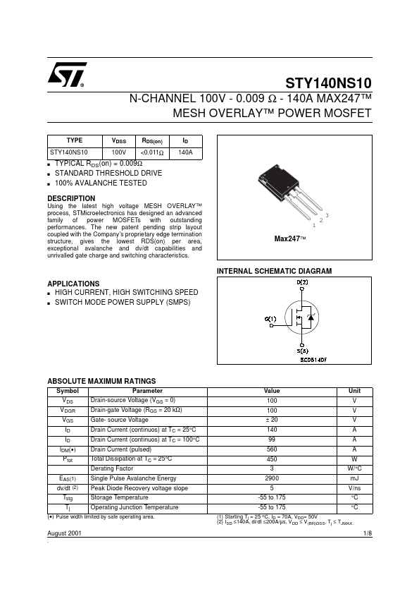
2 1 3
Max247™
INTERNAL SCHEMATIC DIAGRAM APPLICATIONS s HIGH CURRENT, HIGH SWITCHING SPEED s SWITCH MODE POWER SUPPLY (SMPS)
ABSOLUTE MAXIMUM RATINGS
Symbol VDS VDGR VGS ID ID IDM(- ) Ptot EAS(1) dv/dt (2) Tstg Tj Parameter Drain-source Voltage (VGS = 0) Drain-gate Voltage (RGS = 20 kΩ) Gate- source Voltage Drain Current (continuos) at TC = 25°C Drain Current (continuos) at TC = 100°C Drain Current (pulsed) Total Dissipation at TC = 25°C Derating Factor Single Pulse Avalanche Energy Peak Diode Recovery voltage slope Storage Temperature Operating Junction Temperature Value 100 100 ± 20 140...