STY16NA90
DESCRIPTION
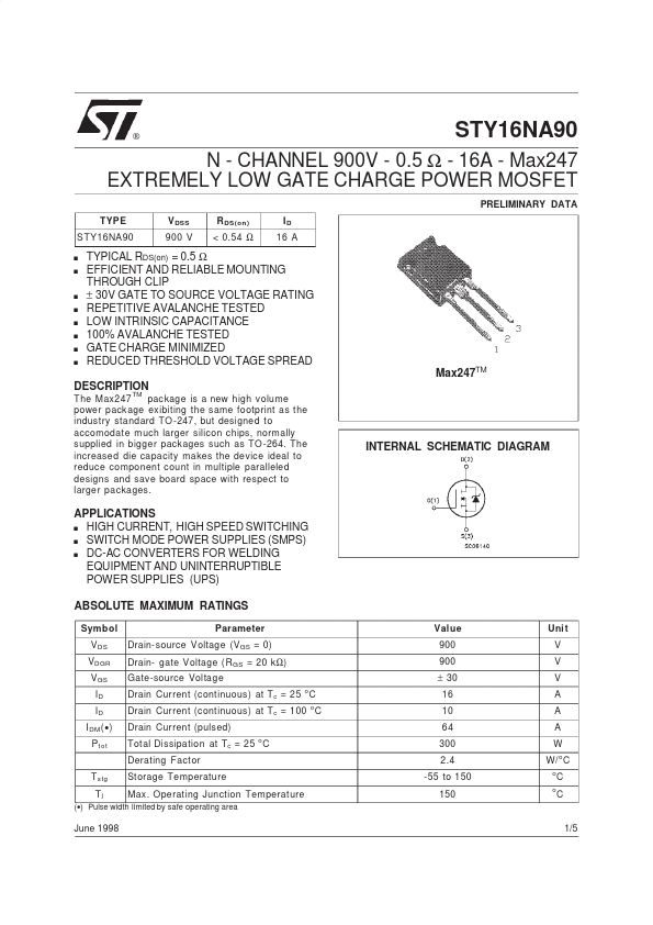
T he Max247 package is a new high volume power package exibiting the same footprint as the industry standard TO -247, but designed to acodate much larger silicon chips, normally supplied in bigger packages such as TO -264. The increased die capacity makes the device ideal to reduce ponent count in multiple paralleled designs and save board space with respect to larger packages.
INTERNAL SCHEMATIC DIAGRAM
APPLICATIONS s HIGH CURRENT, HIGH SPEED SWITCHING s SWITCH MODE POWER SUPPLIES (SMPS) s DC-AC CONVERTERS FOR WELDING EQUIPMENT AND UNINTERRUPTIBLE POWER SUPPLIES (UPS) ABSOLUTE MAXIMUM RATINGS
Symbol V DS VDGR V GS ID ID I DM (
- ) P t ot Parameter Drain-source Voltage (V GS = 0) Drain- gate Voltage (R GS = 20 k Ω) Gate-source Voltage Drain Current (continuous) at T c = 25 o C Drain Current (continuous) at T c = 100 o C Drain Current (pulsed) Total Dissipation at Tc = 25 C Derating Factor T stg Tj St orage Temperature Max. Operating Junction Temperature o
Value 900 900...