STB40N60M2
Features
Order codes VDS @ TJmax RDS(on) max ID
STB40N60M2 STP40N60M2
650 V
0.088 Ω 34 A
STW40N60M2
- Extremely low gate charge
- Lower RDS(on) x area vs previous generation
- Low gate input resistance
- 100% avalanche tested
- Zener-protected
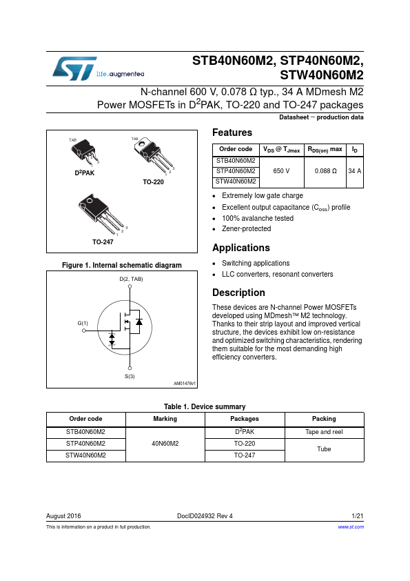
Figure 1. Internal schematic diagram
'7$%
Applications
- Switching applications
- LLC converters, resonant converters
Description
- 6
AM01476v1
These devices are N-channel Power MOSFETs developed using a new generation of MDmesh™ technology: MDmesh II Plus™ low Qg. These revolutionary Power MOSFETs associate a vertical structure to the pany's strip layout to yield one of the world's lowest on-resistance and gate charge. They are therefore suitable for the most demanding high efficiency converters.
Order codes STB40N60M2 STP40N60M2 STW40N60M2
Table 1. Device summary
Marking
Package
D PAK
40N60M2
TO-220
TO-247
Packaging Tape and reel
Tube
May 2014
This is information on a product in full production.
Doc ID024932...