SDM9410
( Data Sheet : .. )
S DM9410
S am Hop Microelectronics C orp.
P R E LIMINAR Y
N-C hannel E nhancement Mode Field E ffect Transistor
P R ODUC T S UMMAR Y
V DS S
30V
F E AT UR E S
( m W ) MAX
7A
R DS (ON)
S uper high dense cell design for low R DS (ON ).
30 @ V G S = 10V 50 @ V G S = 4.5V
R ugged and reliable. S urface Mount P ackage.
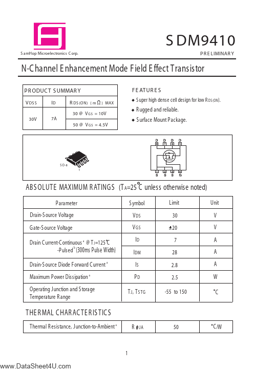
S O-8 1
ABS OLUTE MAXIMUM R ATINGS (T A=25 C unless otherwise noted)
P arameter Drain-S ource Voltage Gate-S ource Voltage Drain C urrent-C ontinuous a @ T J =125 C b -P ulsed (300ms Pulse Width) Drain-S ource Diode Forward C urrent a Maximum P ower Dissipation a Operating Junction and S torage Temperature R ange S ymbol V DS V GS ID IDM IS PD T J , T S TG Limit 30 20 7 28 2.8 2.5 -55 to 150 Unit V V A A A W C
THE R MAL C HAR AC TE R IS TIC S
Thermal R esistance, Junction-to-Ambient a R JA 50 C /W
..
..
S DM9410
E LE CTR ICAL CHAR ACTE R IS TICS (T A =25 C unless otherwise noted)
Parameter OFF CHAR ACTE R IS TICS
Drain-S ource Breakdown...