Datasheet Details
| Part number | KB8821 |
|---|---|
| Manufacturer | Samsung |
| File Size | 237.48 KB |
| Description | FREQUENCY SYNTHESIZER |
| Datasheet |
 KB8821_Samsungsemiconductor.pdf KB8821_Samsungsemiconductor.pdf
|
| Part number | KB8821 |
|---|---|
| Manufacturer | Samsung |
| File Size | 237.48 KB |
| Description | FREQUENCY SYNTHESIZER |
| Datasheet |
KB8821_Samsungsemiconductor.pdf
|
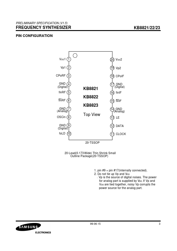
Pin No 1 Symbol VDD1 I/O Description KB8821/22/23 Power supply voltage input for the RF PLL part.V DD1 must equal VDD2. In order to reject supply noise, bypass capacitors must be placed as close as possible to this pin and be connected directly to the ground plane.Power supply voltage input for RF charge pump(≥ VDD1).Internal RF charge pump output for connection to an external loop filter whose filtered output drives an external VCO.Ground for RF digital blocks.RF prescaler input.The sig
📁 KB8821 Similar Datasheet