Description
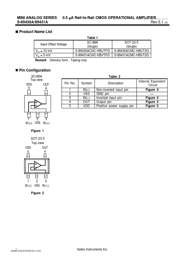
Non-inverted input pin GND pin Inverted input pin Output pin Positive power supply pin Internal Equivalent Circuit Figure ⎯ Figure Figure Figure 4 4 3 5
+
3 1 2 IN (+) VSS IN (
)
Figure 1
SOT-23-5 Top view OUT VDD 4 5 +
1 2 3 IN (+) VSS IN (
)
Figure 2
2
Seiko Instruments Inc.MINI ANALOG SERIES Rev.5.1_00
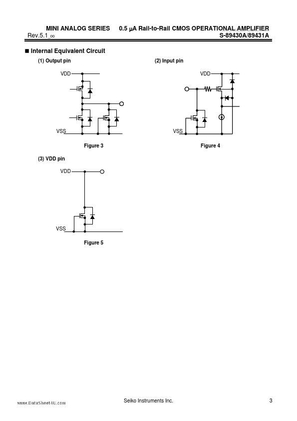
Internal Equivalent Circuit
(1) Output pin
VDD
0.5 μA Rail-to-Rail CMOS OPERATIONAL AMPLIFIER www.DataSheet4U.com S-89430A/89431A
(2) In
Features
- y Lower operating voltage than the conventional general-purpose operational amplifiers: VDD = 0.9 to 5.5 V y Low current consumption: y Wide I/O voltage range: ( Rail-to-Rail ) y Low input offset voltage: 10.0 mV (max. ) (S-89430A) 5.0 mV (max. ) (S-89431A) y No external capaciters required for internal phase compensation y Lead-free products IDD = 0.5 μA VCMR = VSS to VDD.
 S-89430A_SeikoInstruments.pdf