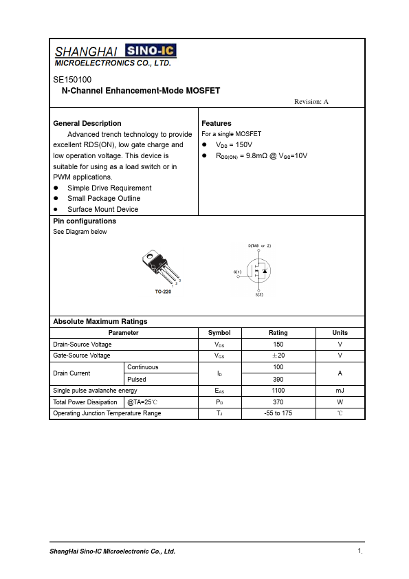
Description
Advanced trench technology to provide
excellent RDS(ON), low gate charge and low operation voltage.This device is suitable for using as a load switch or in PWM applications.
Simple Drive Requirement
Small Package Outline
Surface Mount Device
Pin configurations
See Diagram below
Features
- For a single MOSFET.
- VDS = 150V.
- RDS(ON) = 9.8mΩ @ VGS=10V
Absolute Maximum Ratings
Parameter
Drain-Source Voltage
Gate-Source Voltage
Drain Current
Continuous Pulsed
Single pulse avalanche energy
Total Power Dissipation @TA=25℃
Operating Junction Temperature Range
Symbol VDS VGS
ID
EAS PD TJ
Rating 150 ±20 100 390 1100 370
-55 to 175
Units V V
A
mJ W ℃
ShangHai Sino-IC Microelectronic Co. , Ltd. 1.
SE150100
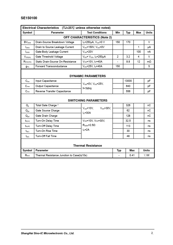
Electrical Characteristics (TJ=25℃ unless otherwise noted)
Sym.
 SE150100-Sino-IC.pdf