Datasheet Details
- Part number
- TC7SP302WBG
- Manufacturer
- Toshiba ↗ Semiconductor
- File Size
- 277.36 KB
- Datasheet
- TC7SP302WBG_ToshibaSemiconductor.pdf
- Description
- Dual supply 2-Input NOR Gate
TC7SP302WBG Description
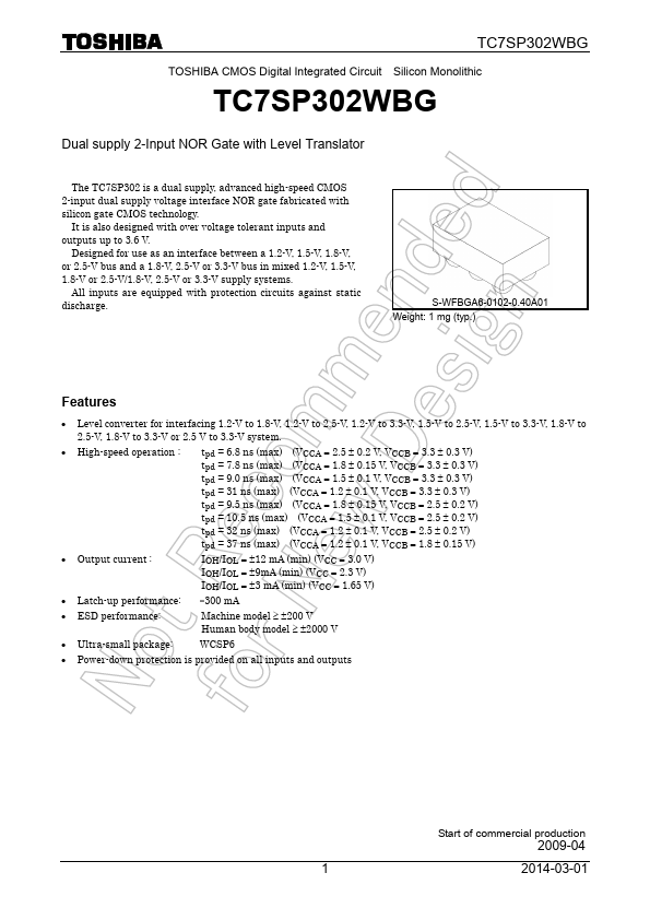
TC7SP302WBG TOSHIBA CMOS Digital Integrated Circuit Silicon Monolithic TC7SP302WBG Dual supply 2-Input NOR Gate with Level Translator The TC7SP302 is.
TC7SP302WBG Features
* Level converter for interfacing 1.2-V to 1.8-V, 1.2-V to 2.5-V, 1.2-V to 3.3-V, 1.5-V to 2.5-V, 1.5-V to 3.3-V, 1.8-V to 2.5-V, 1.8-V to 3.3-V or 2.5 V to 3.3-V system.
* High-speed operation :
tpd = 6.8 ns (max) (VCCA = 2.5 ± 0.2 V, VCCB = 3.3 ± 0.3 V) tpd = 7.8 ns (max) (VCCA
📁 Related Datasheet
📌 All Tags
TC7SP302WBG Stock/Price