TA8227P
Features
- High power
: Pout = 2.5 W/CH (typ.) (VCC = 9 V, RL = 4 Ω, f = 1 k Hz, THD = 10%)
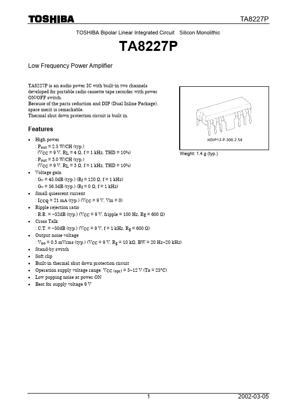
Weight: 1.4 g (typ.)
: Pout = 3.0 W/CH (typ.) (VCC = 9 V, RL = 3 Ω, f = 1 k Hz, THD = 10%)
- Voltage gain
: Gv = 45.0d B (typ.) (Rf = 120 Ω, f = 1 k Hz)
: Gv = 56.5d B (typ.) (Rf = 0 Ω, f = 1 k Hz)
- Small quiescent current
: ICCQ = 21 m A (typ.) (VCC = 9 V, Vin = 0)
- Ripple rejection ratio
: R.R. =
- 52d B (typ.) (VCC = 9 V, fripple = 100 Hz, Rg = 600 Ω)
- Cross Talk
: C.T. =
- 50d B (typ.) (VCC = 9 V, f = 1 k Hz, Rg = 600 Ω)
- Output noise voltage
: Vno = 0.3 m Vrms (typ.) (VCC = 9 V, Rg = 10 kΩ, BW = 20 Hz~20 k Hz)
- Stand-by switch
- Soft clip
- Built-in thermal shut down protection circuit
- Operation supply voltage range: VCC (opr) = 5~12 V (Ta = 25°C)
- Low popping noise at power ON
- Best for supply voltage 9 V
1 2002-03-05
Block Diagram
Application Information and Application Method
1. Adjustment of voltage gain
The voltage gain Gv is obtained as follows...