TC7WZ00FK Overview
Key Specifications
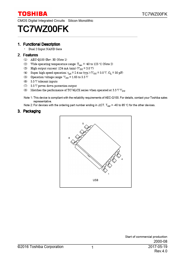
Package: VSSOP
Operating Voltage: 1.8 V
Max Voltage (typical range): 5.5 V
Min Voltage (typical range): 1.65 V
Key Features
- (2) Wide operating temperature range: Topr = -40 to 125 (Note
- Marking and Pin Assignment TC7WZ00FK Marking
- IEC Logic Symbol Pin Assignment (Top view)
- Truth Table A B Y L L H L H H H L H H H L