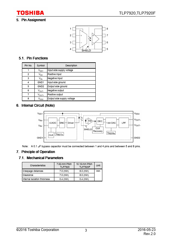
Description
VDD1 VIN+ VINGND1 GND2 VOUTVOUT+ VDD2
Input side supply voltage Positive input Negative input Input side ground Output side ground Negative output Positive output Output side supply voltage
6. Internal Circuit (Note)
TLP7920,TLP7920F
Note: A 0.1 µF bypass capacitor must be connected between 1 and 4 pins and between 5 and 8 pins.7. Principle of Operation 7.1. Mechanical Parameters
Characteristics
Creepage distances Clearance Internal isolation thickness
7.62-mm Pitch TLP7920 7.0 (min) 7.0
Features
- (1) Output side supply voltage: 3.0 to 5.5 V (2) Output side supply current: 6.2 mA (typ. ) (3) Operating temperature range: -40 to 105 (4) Common-mode transient immunity: 15 kV/µs (min) (5) Safety standards
UL-approved: UL1577, File No. E67349 cUL-approved: CSA Component Acceptance Service No.5A File No. E67349 VDE-approved: EN60747-5-5, EN60065 or EN60950-1 (Note 1)
Note 1: When a VDE approved type is needed, please designate the Option (D4). ©2016 Toshiba Corporation
1
Start of commercial p.
 TLP7920-Toshiba.pdf