Description
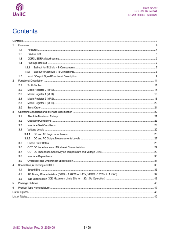
9 2 Functional Description 11 2.1 Truth Tables 11 2.2 Mode Register 0 (MR0) 14 2.3 Mode Register 1 (MR1) 16 2.4 Mode Register 2 (MR2) 18 2.5 Mode Register 3 (MR3) 20 2.6 Burst Order 21 3 Operating Conditions and Interface Specification 22 3.1 Absolute Maximum Ratings 22 3.2 Operating Conditions 23 3.3 Interface Test Conditions 24 3.4 Voltage Levels 25 3.4.1 DC and AC Logic Input Levels 25 3.4.2 DC and AC Output Measurements Levels 27 3.5 Output Slew R
Features
- 4 1.2 Product List 5 1.3 DDR3L SDRAM Addressing 6 1.4 Package Ball out 7
1.4.1 Ball out for 512 Mb × 8 Components 7 1.4.2 Ball out for 256 Mb ×16 Components 8 1.5 Input / Output Signal Functional.


