SI8401DB
FEATURES
- Trench FET® power MOSFET
- MICRO FOOT® chipscale packaging reduces footprint area profile (0.62 mm) and on-resistance per footprint area
- Pin patible to industry standard Si3443DV
- Material categorization: for definitions of pliance please see .vishay./doc?99912
APPLICATIONS
- PA, battery, and load switch
- Battery charger switch
- PA switch
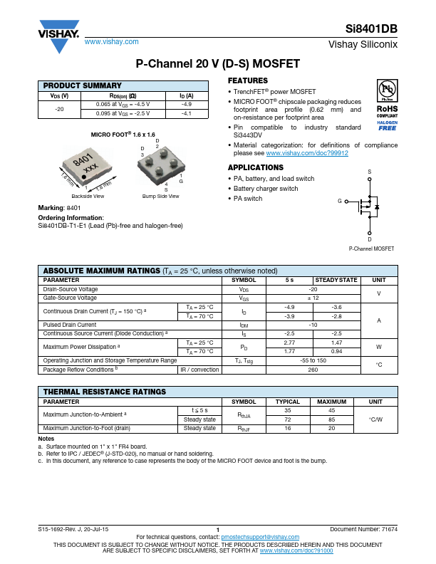
D P-Channel MOSFET
ABSOLUTE MAXIMUM RATINGS (TA = 25 °C, unless otherwise noted)
PARAMETER
SYMBOL
Drain-Source Voltage
Gate-Source Voltage
Continuous Drain Current (TJ = 150 °C) a Pulsed Drain Current
TA = 25 °C TA = 70 °C
Continuous Source Current (Diode Conduction) a
Maximum Power Dissipation a Operating Junction and Storage Temperature Range
TA = 25 °C TA = 70 °C
Package Reflow Conditions b
IR / convection
VDS VGS
IDM IS
TJ, Tstg
5s
STEADY STATE
-20
± 12
-4.9
-3.6
-3.9
-2.8
-10
-2.5
-2.5...