Si8406DB
FEATURES
- Trench FET® power MOSFET
- Ultra-small 1.5 mm x 1 mm maximum outline
- Ultra-thin 0.59 mm maximum height
- Material categorization: for definitions of pliance please see .vishay./doc?99912
APPLICATIONS
- Load switch
- Battery management
- Boost converter
Available
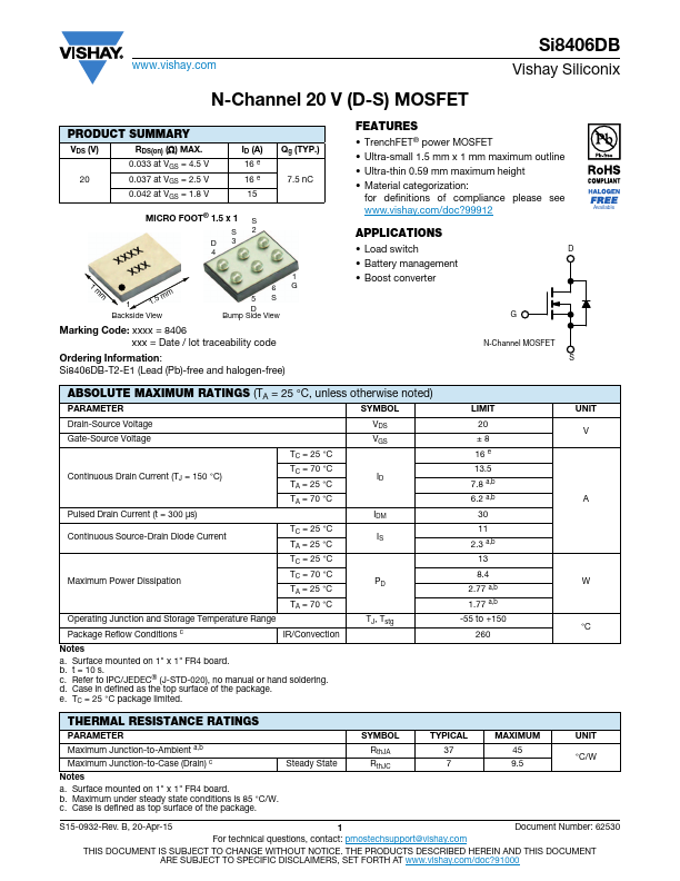
N-Channel MOSFET S
ABSOLUTE MAXIMUM RATINGS (TA = 25 °C, unless otherwise noted)
PARAMETER
SYMBOL
Drain-Source Voltage
Gate-Source Voltage
Continuous Drain Current (TJ = 150 °C) Pulsed Drain Current (t = 300 μs)
TC = 25 °C TC = 70 °C TA = 25 °C TA = 70 °C
Continuous Source-Drain Diode Current Maximum Power Dissipation Operating Junction and Storage Temperature Range
TC = 25 °C TA = 25 °C TC = 25 °C TC = 70 °C TA = 25 °C TA = 70 °C
Package Reflow Conditions c
IR/Convection
VDS VGS ID IDM IS
PD TJ, Tstg
Notes a. Surface mounted on 1" x 1" FR4 board. b. t = 10 s. c. Refer to IPC/JEDEC® (J-STD-020), no manual or hand soldering. d. Case in defined as the top surface of the package. e. TC = 25 °C...