EAB450M12XM3
Features
- High Power Density Footprint
- High Junction Temperature (175 °C) Operation
- Low Inductance (6.7 n H) Design
- Implements Conduction-Optimized Third
Generation Si C MOSFET Technology
- Silicon Nitride Insulator and Copper Baseplate
- 1200 V Drain-Source Voltage
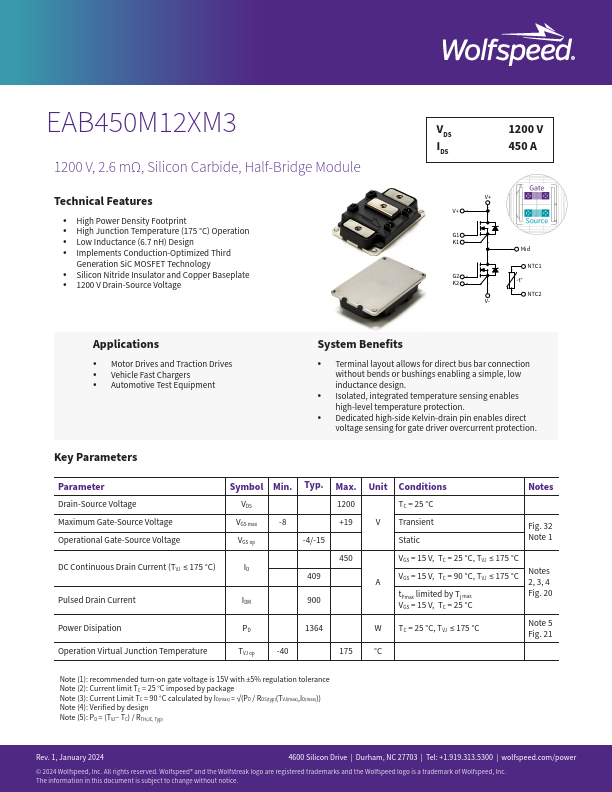
V+ V+
G1 K1
G2 K2
V-
Mid
NTC1 -t°
NTC2
Applications
- Motor Drives and Traction Drives
- Vehicle Fast Chargers
- Automotive Test Equipment
System Benefits
3 8,9
- Terminal layout allows for direct bus bar connection w Bithout bends or bushings inductance design. enab4ling
5 a simple, low
- Isolated, integrated temperature sensing enables high-level temperature protection.
- Dedicated high-side Kelvin-drain67 pin enables dire-tc°t voltage sensing for gate driver overcurrent protectio1n1 .
Key Parameters
Parameter
Symbol Min. Typ. Max. Unit Conditions
Notes
Drain-Source Voltage Maximum Gate-Source Voltage Operational Gate-Source Voltage
VDS VGS max VGS op
TC = 25...