Datasheet Details
| Part number | XD272 |
|---|---|
| Manufacturer | XINLUDA |
| File Size | 375.26 KB |
| Description | dual operational amplifiers |
| Datasheet |
 XD272-XINLUDA.pdf XD272-XINLUDA.pdf
|
| Part number | XD272 |
|---|---|
| Manufacturer | XINLUDA |
| File Size | 375.26 KB |
| Description | dual operational amplifiers |
| Datasheet |
XD272-XINLUDA.pdf
|
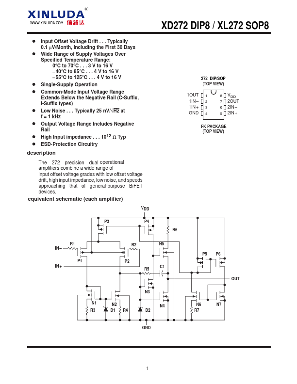
The 272 precision dual operational amplifiers combine a wide range of input offset voltage grades with low offset voltage drift, high input impedance, low noise, and speeds approaching that of general-purpose BiFET devices.equivalent schematic (each amplifier) VDD P3 P4 XD272 DIP8 / XL272 SOP8 272 DIP/SOP (TOP VIEW) 1OUT 1 1IN 2 1IN + 3 GND 4 8 VDD 7 2OUT 6 2IN 5 2IN + FK PACKAGE (TOP VIEW) R6 R1 IN P1 IN + R2 N5 P2 R5 C1 P5 P6 OUT N1 N2 R3 D1 R4