Datasheet Details
| Part number | YAS539-PZE2 |
|---|---|
| Manufacturer | YAMAHA |
| File Size | 924.35 KB |
| Description | LSI |
| Datasheet |
 YAS539-PZE2-YAMAHA.pdf YAS539-PZE2-YAMAHA.pdf
|
|
|
The YAS539-PZE2 by YAMAHA is a LSI. Below is the official datasheet preview.
| Part number | YAS539-PZE2 |
|---|---|
| Manufacturer | YAMAHA |
| File Size | 924.35 KB |
| Description | LSI |
| Datasheet |
YAS539-PZE2-YAMAHA.pdf
|
|
|
|
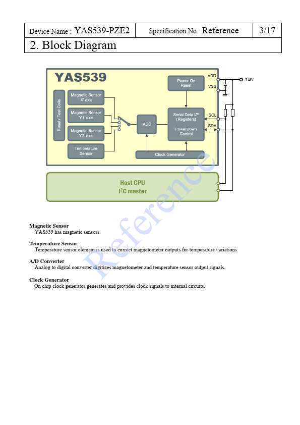
Pin Arrangement rence Pin Descriptions fe Ball No.Name I/O e 1A SCL Is R 1B VDD - Description I2C serial clock Power (1.8 V typ.) 2A SDA Is/Od I2C serial data 2B VSS - Ground Is : Schmitt trigger input Od : Open-drain outpu Device Name : YAS539-PZE2 Specification No.:Reference 5/17 4. Electrical Characteristics Absolute Maximum Ratings Parameter Supply Voltage (VDD) Digital Input Pin Voltage (SCL, SDA) Storage Temperature Maximum Applicable Magnetic Field Intensit
📁 YAS539-PZE2 Similar Datasheet