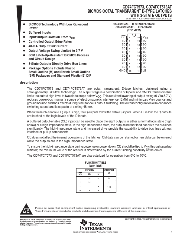
CD74FCT573AT
description
The CD74FCT573 and CD74FCT573AT are octal, transparent, D-type latches, designed using a small-geometry Bi CMOS technology. The output stage is a bination of bipolar and CMOS transistors that limits the output high level to two diode drops below VCC. This resultant lowering of output swing (0 V to 3.7 V) reduces power-bus ringing [a source of electromagnetic interference (EMI)] and minimizes VCC bounce and ground bounce and their effects during simultaneous output switching. The output configuration also enhances switching speed and is capable of sinking 48 m A.
When the latch-enable (LE) input is high, the Q outputs follow the data (D) inputs. When LE is low, the Q outputs are latched at the logic levels of the D inputs.
A buffered output-enable (OE) input can be used to place the eight outputs in either a normal logic state (high or low) or a high-impedance state. In the high-impedance state, the outputs neither load nor drive the bus lines significantly. The...