CDCLVD1204
Features
- 1 2:4 Differential Buffer
- Low Additive Jitter: <300 fs RMS in 10-k Hz to
20-MHz
- Low Output Skew of 20 ps (Maximum)
- Universal Inputs Accept LVDS, LVPECL, and
LVCMOS
- Selectable Clock Inputs Through Control Pin
- 4 LVDS Outputs, ANSI EAI/TIA-644A Standard patible
- Clock Frequency: Up to 800 MHz
- Device Power Supply: 2.375 V to 2.625 V
- LVDS Reference Voltage, VAC_REF, Available for
Capacitive Coupled Inputs
- Industrial Temperature Range:
- 40°C to 85°C
- Packaged in 3 mm × 3 mm, 16-Pin VQFN (RGT)
- ESD Protection Exceeds 3 k V HBM, 1 k V CDM
2 Applications
- Telemunications and Networking
- Medical Imaging
- Test and Measurement Equipment
- Wireless munications
- General Purpose Clocking
3 Description
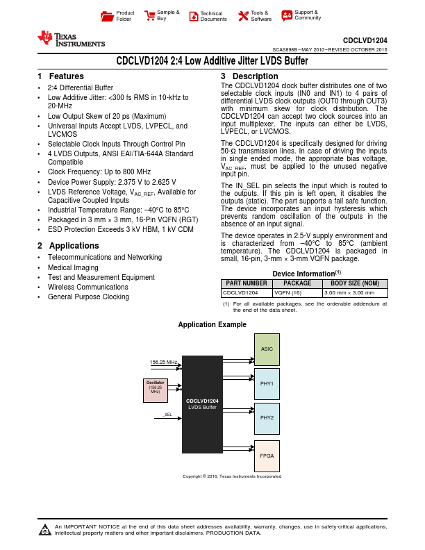
The CDCLVD1204 clock buffer distributes one of two selectable clock inputs (IN0 and IN1) to 4 pairs of differential LVDS clock outputs (OUT0 through OUT3) with minimum skew for clock distribution. The CDCLVD1204 can accept two clock sources into an input multiplexer. The...