Datasheet4U Logo Datasheet4U.com

CDCS504-Q1 Datasheet - Texas Instruments

CDCS504-Q1 Clock Buffer and Clock Multiplier

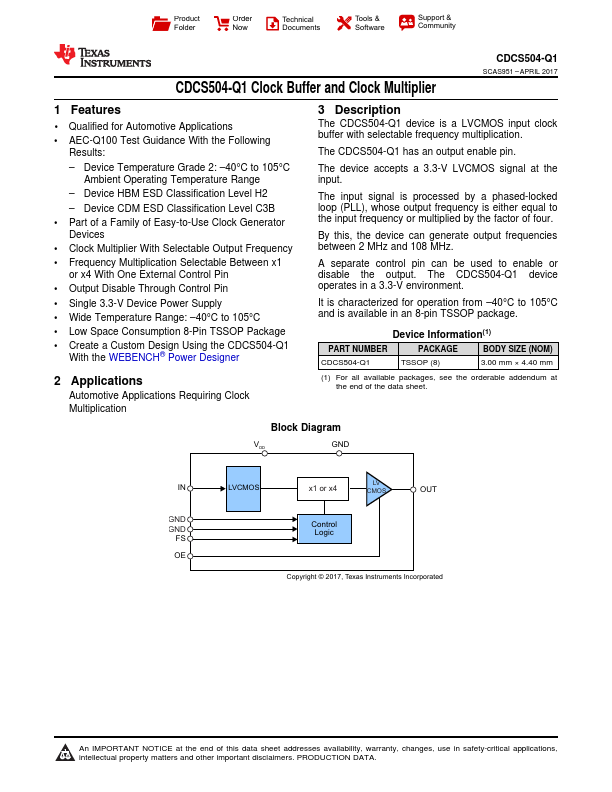
The CDCS504-Q1 device is a LVCMOS input clock buffer with selectable frequency multiplication. The CDCS504-Q1 has an output enable pin. The device accepts a 3.3-V LVCMOS signal at the input. The input signal is processed by a phased-locked loop (PLL), whose output frequency is either equal to the in.

CDCS504-Q1 Features

* 1 Qualified for Automotive Applications

* AEC-Q100 Test Guidance With the Following Results:

* Device Temperature Grade 2:

* 40°C to 105°C Ambient Operating Temperature Range

* Device HBM ESD Classification Level H2

* Device CDM ESD Classification Leve

CDCS504-Q1 Datasheet (633.88 KB)

Preview of CDCS504-Q1 PDF
CDCS504-Q1 Datasheet Preview Page 2 CDCS504-Q1 Datasheet Preview Page 3

Datasheet Details

Part number:

CDCS504-Q1

Manufacturer:

Texas Instruments ↗

File Size:

633.88 KB

Description:

Clock buffer and clock multiplier.

📁 Related Datasheet

CDCS501 SSC Clock Generator/Buffer (Texas Instruments)

CDCS502 Crystal Oscillator / Clock Generator (Texas Instruments)

CDCS503 Clock Buffer/Clock Multiplier (Texas Instruments)

CDCS503-Q1 Clock Buffer/Clock Multiplier (Texas Instruments)

CDC-Z137 FM / AM CD Player (Aiwa)

CDC1104 1 to 4 Configurable Clock Buffer (Texas Instruments)

CDC111 1-LINE TO 9-LINE DIFFERENTIAL LVPECL CLOCK DRIVER (Texas Instruments)

CDC1607F-E Automotive Controller Specification (Micronas)

TAGS

CDCS504-Q1 Clock Buffer and Clock Multiplier Texas Instruments

CDCS504-Q1 Distributor