SN74HCT00N
Features
- Operating voltage range of 4.5V to 5.5V
- Outputs can drive up to 10 LSTTL loads
- Low power consumption, 20-μA max ICC
- Typical tpd = 10ns
- ±4-m A output drive at 5V
- Low input current of 1μA max
- Inputs are TTL-voltage patible x A
2 Description
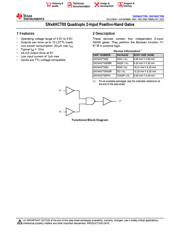
These devices contain four independent 2-input NAND gates. They perform the Boolean function Y= A
- B in positive logic.
Device Information(1)
PART NUMBER
PACKAGE BODY SIZE (NOM)
SN74HCT00D
SOIC (14)
8.65 mm × 3.90 mm
SN74HCT00DBR SSOP (14) 6.20 mm × 5.30 mm
PDIP (14)
19.31 mm × 6.35 mm
SN74HCT00NSR SO (14)
10.20 mm × 5.30 mm
SN74HCT00PW
TSSOP (14) 5.00 mm × 4.40 mm
(1) For all available packages, see the orderable addendum at the end of the data sheet. x Y x B
Functional Block Diagram
An IMPORTANT NOTICE at the end of this data sheet addresses availability, warranty, changes, use in safety-critical applications, intellectual property matters and other important disclaimers. PRODUCTION DATA.
SN54HCT00...