Datasheet Details
| Part number | 74LV595D |
|---|---|
| Manufacturer | nexperia |
| File Size | 274.53 KB |
| Description | 8-bit serial-in/serial-out or parallel-out shift register |
| Datasheet |
 74LV595D Datasheet 74LV595D Datasheet
|
|
|
This page provides the datasheet information for the 74LV595D, a member of the 74LV595 8-bit serial-in/serial-out or parallel-out shift register family.
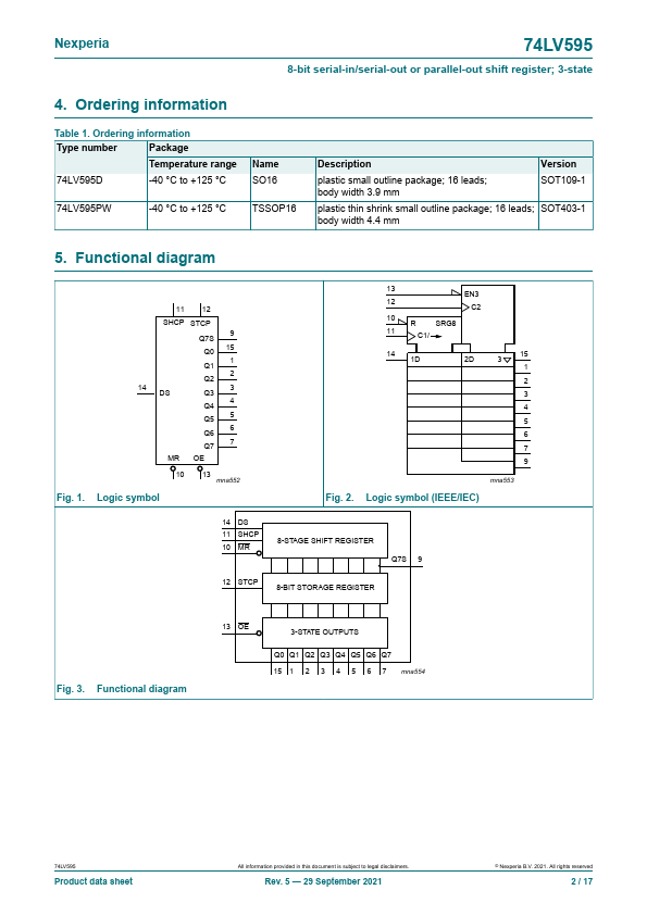
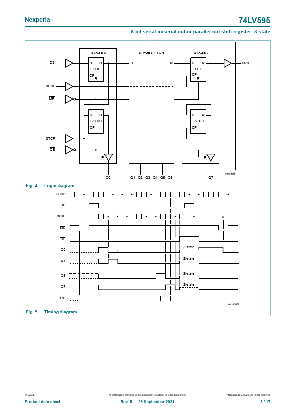
The 74LV595 is an 8-bit serial-in/serial or parallel-out shift register with a storage register and 3-state outputs.
Both the shift and storage register have separate clocks.
| Part number | 74LV595D |
|---|---|
| Manufacturer | nexperia |
| File Size | 274.53 KB |
| Description | 8-bit serial-in/serial-out or parallel-out shift register |
| Datasheet |
74LV595D Datasheet
|
|
|
|