Datasheet Details
| Part number | 74LVT08 |
|---|---|
| Manufacturer | nexperia |
| File Size | 208.66 KB |
| Description | 3.3V Quad 2-input AND gate |
| Datasheet |
 74LVT08 Datasheet 74LVT08 Datasheet
|
|
|
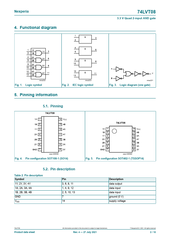
The 74LVT08 is a quad 2-input AND gate.
This device is fully specified for partial power down applications using IOFF.
The IOFF circuitry disables the output, preventing the potentially damaging backflow current through the device when it is powered down.
| Part number | 74LVT08 |
|---|---|
| Manufacturer | nexperia |
| File Size | 208.66 KB |
| Description | 3.3V Quad 2-input AND gate |
| Datasheet |
74LVT08 Datasheet
|
|
|
|