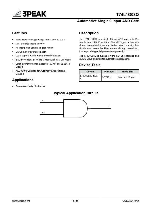
Download T74L1G08Q Datasheet PDF
T74L1G08Q page 2
Page 2
T74L1G08Q page 3
Page 3

T74L1G08Q Key Features

  • Wide Supply Voltage Range from 1.65 V to 5.5 V
  • I/O Tolerance Inputs to 5.5 V
  • All Inputs with Schmitt-Trigger Action
  • CMOS Low Power Dissipation
  • IOFF Supports Partial Power-down Protection
  • ESD Protection: ±4-kV HBM Model, ±1-kV CDM Model
  • Latch-up Performance Exceeds 100 mA per JESD 78
  • AEC-Q100 Qualified for Automotive

T74L1G08Q Description

Wide Supply Voltage Range from 1.65 V to 5.5 V I/O Tolerance Inputs to 5.5 V All Inputs with Schmitt-Trigger Action CMOS Low Power Dissipation IOFF Supports Partial Power-down Protection ESD Protection: Schmitt-Trigger action with slower rise-and-fall times and better noise immunity. IOFF circuits can prevent backflow current during power-down, thus supporting partial power-down protection.